High-NA lithography: a $380M machine with half the field
Four chip giants are preparing to replace an engraving standard in place since the 1980s. The reason is a constraint of optics: to print finer, the 380 million dollar machines cover half the area in a single shot. Artificial intelligence chips, the largest of all, no longer fit.

The fact
On 8 September 2026, ASML and TSMC launched an industry initiative to move lithography onto a 6 by 12-inch photomask, twice as long as the 6-inch format in place since the 1980s. Samsung joined the same day; Intel Foundry has championed it for three years. Pilot line in 2031, production in 2033. The 6-inch mask stays the production format. Behind that workshop detail sits a constraint: the most expensive machines ever built, around 380 million dollars each, cannot print the largest chips in a single shot.
Why it deserves attention
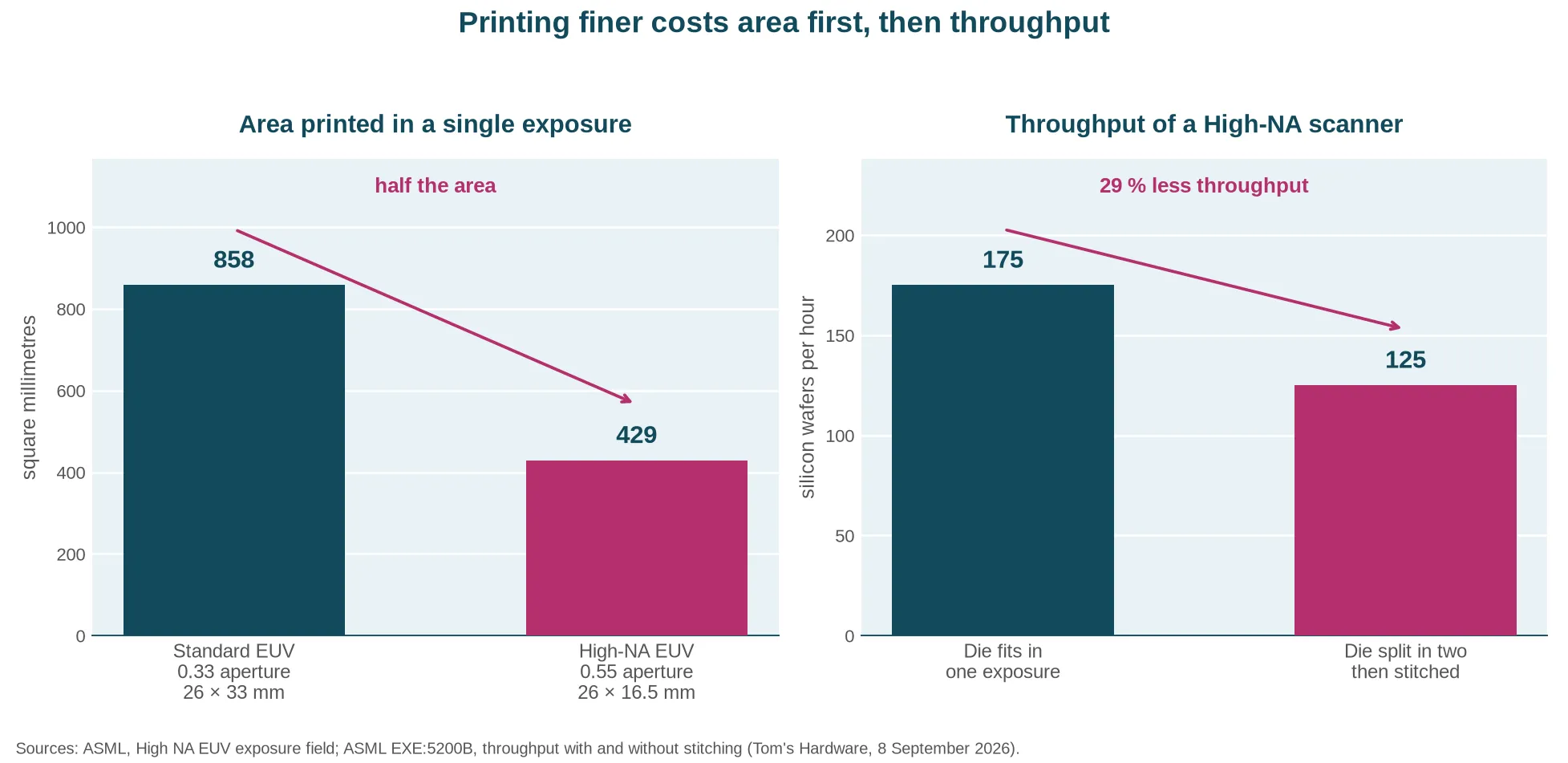
Printing finer means opening the optics wider: numerical aperture rises from 0.33 to 0.55. But optics never win on both counts: to keep the incoming and reflected beams from overlapping on the mask, ASML had to shrink the image twice as hard in one direction as in the other. The area printed in a single exposure therefore falls from 26 by 33 millimetres to 26 by 16.5: half of it. No software brings it back: it is a law of optics.
Yet the chips that need that fineness most, artificial intelligence accelerators, are also the largest. They no longer fit in one exposure. They must be cut in two, the wafer exposed twice, then the seam aligned to within a nanometre. On the EXE:5200B, ASML’s production High-NA scanner, that stitching drops throughput from 175 to 125 wafers an hour.
The stake sits in those 29 % lost. A 380 million dollar machine running at 71 % of its rated pace makes every chip leaving it more expensive. One foundry carries that bill today, Intel; TSMC is aiming at 2030, Samsung at 2028 for memory. The cost will then travel up to the price of AI servers rented everywhere. The fix is exactly that mask twice as long: an entire mask-making supply chain to rebuild. Seven years, at best.
To understand why a handful of players decide how fine the world’s chips can be, read the Fundamental: “Semiconductors: technology and geopolitics.”
You will learn how the chain splits from design to packaging, why ASML holds a monopoly on EUV lithography, and a four-question grid for placing any chip news you read.
Read the Fundamental →